|
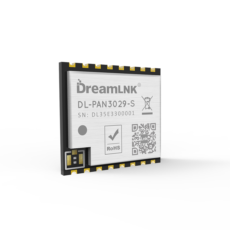
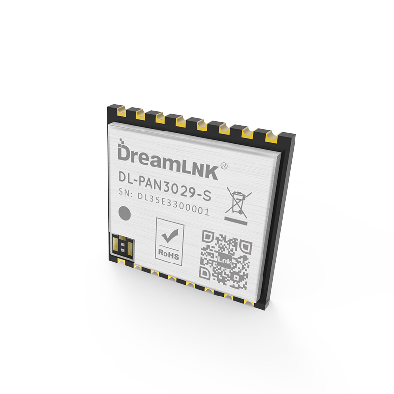


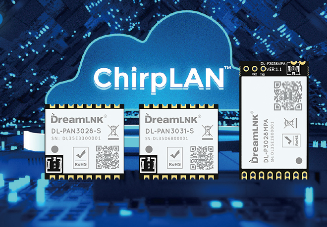
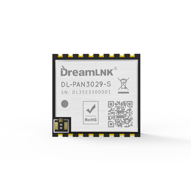
DL-PAN3029-S
DreamLNK/骏晔
DL-PAN3029-S
433MHz/868MHz/915MHz
PAN3029
20dBm
2.0~3.6V
-141dBm
3000m
17.1*16.1*2.5mm
| Quantity: | |
|---|---|
Brief Introduction
DL-PAN3029-S is a wireless module designed based on PANCHIP’s radio frequency chip PAN3029. The power supply of this module adopts a chip integrated DCDC working mode, which can greatly reduce power consumption in various modes. It is equipped with a built-in temperature compensation crystal, which can effectively reduce temperature drift and ensuring more stable transmission. This Wireless Module is compact in size, and has the characteristics of ultra-low receiving power consumption, strong anti-interference ability, and longer transmission distance.
Moreover, DL-PAN3029-S RF module adopts the new generation Chirp IoT ™ Modulation technology, which has strong anti-interference ability and long communication range. The TX power can be configured through software, and the maximum TX power can reach +20dBm. It also has a high sensitivity of -141dBm and a receiving current of less than 5.9mA, when it works as a receiver. The frame structure of this RF chip has added MAPM function, allowing data frames received from addresses other than their own to be directly discarded and enter sleep mode, which can further optimize the device power consumption at the receiver end.
Compared with traditional modulation technology, Chirp-IoT ™ Modulation technology has obvious advantages in adjustable bandwidth, spread spectrum factor and error correction rate, which solves the problem of distance, anti-interference and power consumption that traditional design schemes cannot take into account at the same time. It can be widely used in various wireless communication fields of the IoT industry, especially battery powered applications, as well as long-distance communication projects.
Features
● Chirp-IoT ™ modulation technology;
● It supports frequency range of 408~565MHz; 816~1080MHz;
● Designed frequency (use recommended frequency to achieve the best RF performance): 408~565MHz --> 433M module; 816~1080MHz --> 868/915M module;
● The working voltage is 2.0~3.6V, use stable voltage (≥2.4V) to maximum output power;
● Supported bandwidth: 62.5KHz, 125KHz, 250KHz, 500KHz;
● Supported spreading factor: SF5/SF6/SF7/SF8/SF9/SF10/SF11/SF12;
● Supported Bit Rates: 4/5, 4/6, 4/7, 4/8;
● Supports fast Channel Activity Detection (CAD);
● Supports low-rate mode;
● Optional passive/temperature compensated crystals;
● Supports 3/4-line SPI configuration interface;
● Operating temperature: -40~85 C.
Download Center
DL-PA3029-S Specification V1.1 
Typical Application
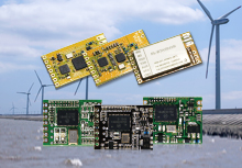
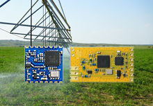
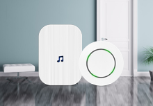
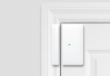
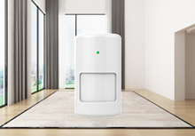
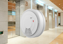
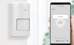
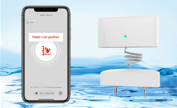
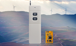
● Wireless automatic meter reading (water meter, electric meter, gas meter)
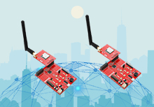
● Ultra-long range data communication
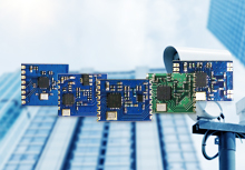
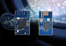
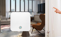
● Smart home system
● Smart building
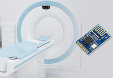
● Industrial controllers, sensors
● Agricultural automation solutions
● Intelligent parking system
● Automotive industry applications
● Supply chain logistics
Technical Parameter
Parameter | Min. | Typical | Max. | Unit | Remarks |
Operating conditions | |||||
Working Voltage (VDD) | 2.0 | 3.3 | 3.6 | V | @DCDC mode 2V~3.6V, to ensure maximum chip power, stable voltage should ≥2.4V |
Communication Level Range | -0.3 | VDD | V | Exceeding this range will damage the chip | |
Working Temperature Range | -40 | 25 | 85 | ℃ | The larger the temperature difference, the greater the bandwidth required for communication |
Current consumption | |||||
Receiving Current | 5 | 5.6 | 5.9 | mA | @DCDC @ Active crystal (default) |
4 | 4.7 | 4.9 | mA | @DCDC @ Passive crystal | |
Transmission Current | 115 | 125 | 145 | mA | @433MHz @DCDC @ANT TX 20dbm |
95 | 110 | 135 | mA | @868MHz @DCDC @ANT 50-ohm impedance; TX 18dbm | |
95 | 110 | 135 | mA | @915MHz @DCDC @ANT 50-ohm impedance; TX 18dbm | |
Sleep Current | 0.1 | 0.5 | 0.7 | uA | Save via register |
RF parameters | |||||
Recommended Frequency (For best performance) | 420 | 433/470 | 490 | MHz | @433MHz RF module |
840 | 868/915 | 930 | MHz | @868MHz/915Mhz RF module | |
Transmit Power Range | -30 | 20 | 20 | dBm | Software configurable |
Receiving Sensitivity | -141 | dBm | @BW=62.5KHz, SF=12 | ||
Payload Rate Range | 0.15 | 62.5 | Kb/s | L: BW:62.5, SF:12, CR:4/5 H: BW:500, SF:5, CR:4/5 | |
Communication Rate Range | 0.04 | 0.04 | 0.04 | Kb/s | @BW:62.5, SF:12, CR:4/5 (Min. Rate) Payload: 10byte Preamble: 8byte |
59.33 | 59.33 | 59.33 | Kb/s | @BW:500, SF:5, CR:4/5 (Max. Rate) Payload: 255byte Preamble: 8byte | |
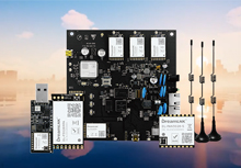
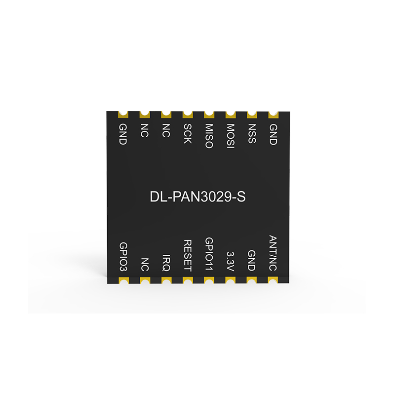
Pin Definitions

No | Definitions | Type | Description |
1 | ANT/NC | AI/AO | RF signal input/output port, π-matching circuit must be reserved; Adopt 50Ω impedance matching for RF routing, route the ground and add via holes around it |
2 | GND | PWR | Reliable grounding |
3 | 3.3V | PWR | Power |
4 | GPIO11 | I/O | Digital I/O port |
5 | RESET | I | Reset pin, effective at low level |
6 | IRQ | O | Interrupt Request Pin, high level active |
7 | NC | No connection | |
8 | GPIO3 | I/O | Digital I/O port |
9 | GND | PWR | Reliable grounding |
10 | NC | No connection | |
11 | NC | No connection | |
12 | SCK | I | SPI Serial Clock Input |
13 | MISO | O | SPI Master Input Slave Output |
14 | MOSI | I | SPI Master Output Slave Input |
15 | NSS | I | SPI Chip Select Input |
16 | GND | PWR | Reliable grounding |
Module Size

Application Connection Diagram

Note: This schematic diagram is for your reference only, it shows the minimum communication connection. The 4-line SPI and IRQ pins need to be connected to the I/O port of the MCU. If you have any question, please contact us for more help.
Typical application
Wireless Data Communication, Wireless Remote Control System; Wireless Alarm & Security Control System; Wireless Sensor Networking, Automatic Data Collection; Industrial Remote Control, Intelligent Control System, Home Automation, Smart Building, Smart Home, Smart City, Telemetry, Automatic (Water, Electricity, Gas) Meter Reading;
Product Tags
RF module, Wireless Module, Wireless Transmitter Module, RF Transmitter Module, 433MHz RF Module, Wireless Transceiver Module, FSK Transceiver module, 433MHz Wireless module, 868MHz Wireless module, 915MHz Wireless module,PANCHIP, Chirp-IoT™